Electron microscopy instrumentation
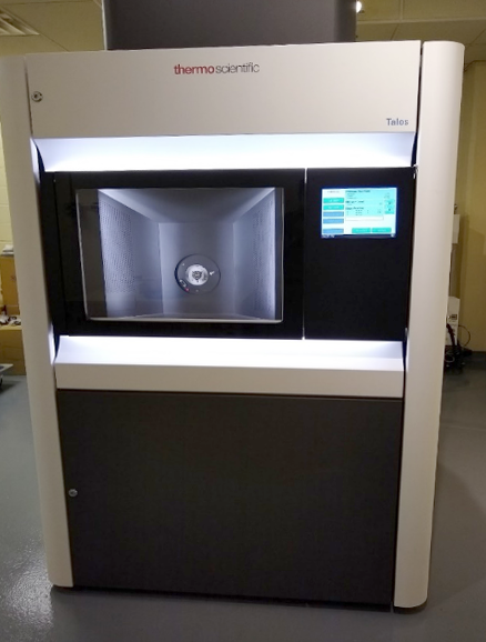
Talos F200X G2 Scanning Transmission Electron Microscope
- Installed and accepted in December 2021
- Equipped with a proprietary "XFEG" high brightness Schottky field emission gun
- Flexible HT range: 20-200 kV with alignments at both 200kV and 80kV
- Resolution: 0.12 nm TEM information limit, 0.16 nm at STEM HAADF
- Four-channel imaging with four STEM detectors (high-angle annular dark field, medium-angle annular dark field, low-angle annular dark field, and bright field)
- Fast EDS elemental mapping with pixel dwell times down to 10 μs
- High speed, large FOV and high sensitivity with Ceta 16M pixels camera
- Precise navigation, drift correction and accuracy with the piezo stage
- TEM/STEM/EDS tomography extends its analytical capabilities to 3D volumes
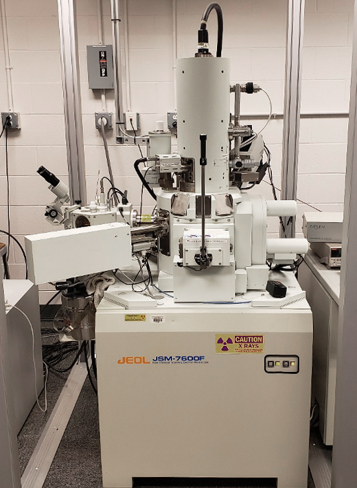
JSM-7600 FE SEM
- Installed in June 2011
- Shottky, field-emission gun with fully automatic control; Accelerating voltage 0.1 to 30 kV
- Practical magnification range: 25 to 1,000,000
- Resolution: 0.8 nm at 30 kV, 1.5 nm at 1 kV, and 5 nm at 100V
- Four electron image signal detectors: In-lens secondary electron detector, Below-the-lens secondary electron detector, Low angle backscatter electron detector and retractable scanning transmitted electron detector
- Equipped with Pegasus Apex 2 integrated EDS and EBSD Systems with capabilities of spectral imaging, OIM data collection and analysis with high accuracy and high efficiency
- A cryo-transfer System (Gatan Alto 2500) allows imaging and analysis of biological and other hydrated specimens
- Motorized 5-axis stage assures precise, reproducible specimen positioning
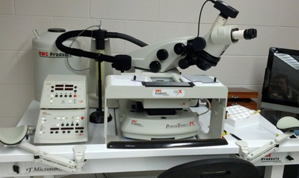
Cryoultramicrotome
- RMC PT-PC
- Polymer materials and biological specimens
- Sections from 10 to 0.005 microns
- Temperature range from -180 °C to +35 °C
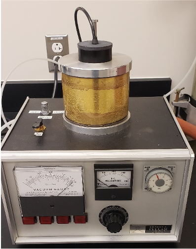
Gold Sputter
- Used to coat non-conductive samples for SEM
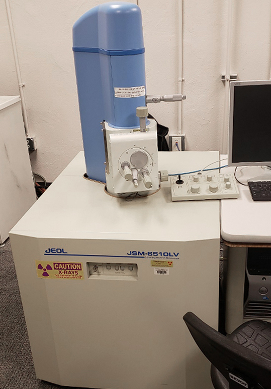
JSM - 6510LV SEM
- Installed in November 2010
- Tungsten emitter; Accelerating voltage 0.5 to 30 kV
- Configured to operate in both high vacuum and low vacuum mode, with the pressure range in low-vacuum mode: 1 to 270 Pa
- Magnification range: 5 to 300,000
- Resolution in high vacuum mode: 3.0 nm at 30 kV and 15 nm at 1 kV (secondary electron image)
- Resolution in low vacuum mode: 4.0 nm at 30 kV (backscatter electron image)
- X-ray energy-dispersive spectrometer (EDS) for elemental spectra, mapping
- Ease of use software and hardware functions and flexibility for the experienced professional or the novice operator.
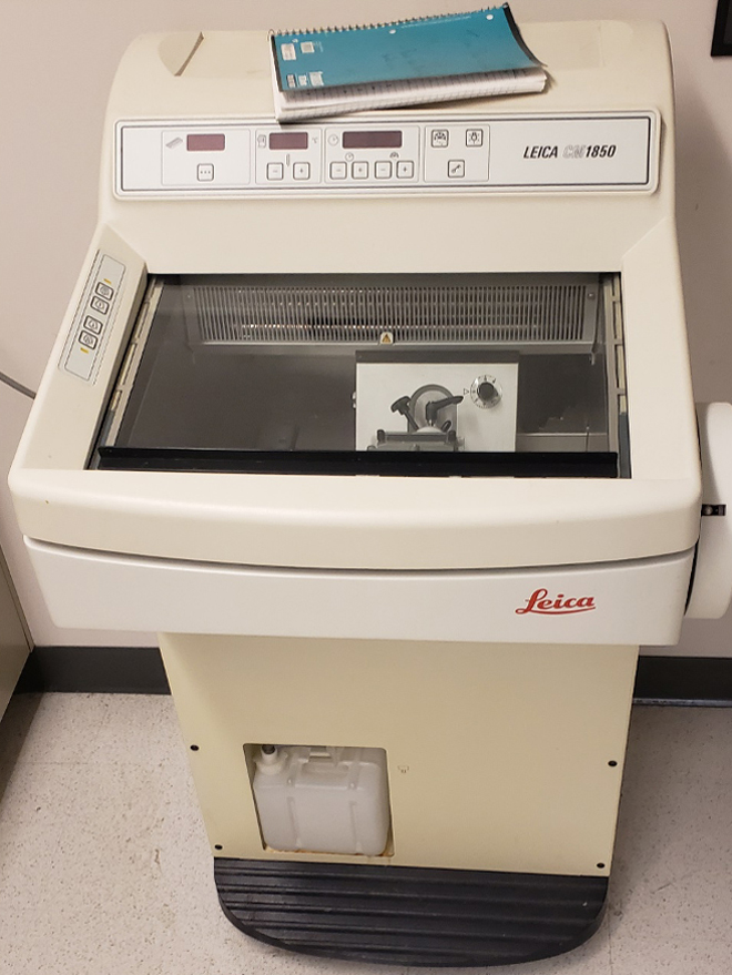
Leica CM1850 Tissue Slicer
- Accurately and reproducibly slices frozen sections from a block of tissue
- Temperature-controlled chamber, down to -35 °C
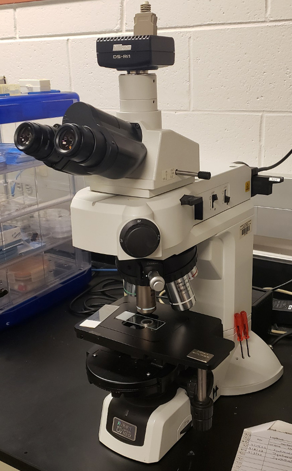
Nikon Eclipse LV100D-U Microscope
- Brightfield and darkfield transmitted and reflected light microscope
- With fluorescence function,
- EX: 450-490 nm, DM: 505 nm, BA: 520 nm
- EX: 510-560 nm, DM: 575 nm, BA: 590 nm
- Objective lenses available, 5x, 10x 20x, 40x, 100x
- Nikon Intensilight C-HGFI Fiber optic light source
- Nikon DS-Ri1 Color Camera (12.7 megapixel CCD)
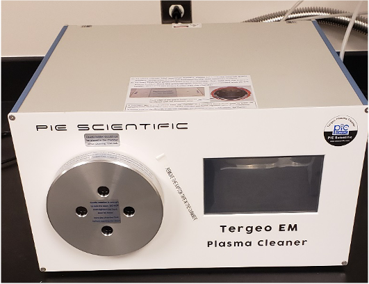
Pie Scientific Tergeo-EM Plasma Cleaner
- Can be used to remove surface oxides and/or hydrocarbon contaminations on TEM samples, to clean TEM sample holders, or to generate hydroxide functional groups on TEM grids using water vapor plasma
- Improves chip bonding for microfluidic devices
- Inner diameter, 110 mm, depth 280 mm
- Maximum power: 75 Watt
- Plasma types available: water vapor and Ar-O2